

Signal acquisition and processing of pressure sensors
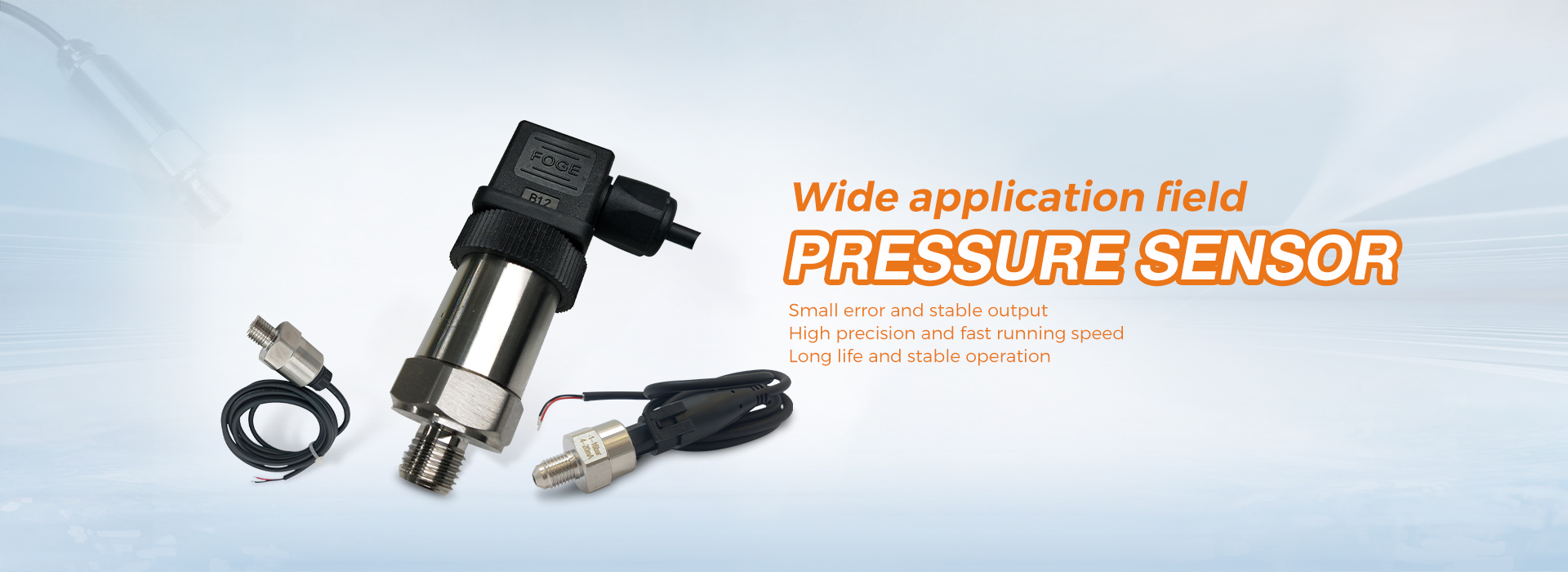
In the field of modern industrial control and system monitoring, it is usually necessary to monitor and measure pressure and weight. Pressure measurement is particularly important as it can be directly used to measure fluids, heights, and other physical quantities. Since loading is an attribute that affects sensor output, pressure and weight measurement devices can be considered as “loading sensors”. The application of load sensors is very extensive, including vacuum gauges to heavy machinery weighing, as well as various fields such as industrial hydraulic equipment and absolute pressure. Each application has different specific requirements for accuracy, precision, and cost. Although there are many methods and techniques for measuring pressure and weight (loading/sensing), the most commonly used measuring device is a stress gauge.
There are two most common types of stress gauges: one is the metal foil commonly used in pressure sensors; Another type is semiconductor based piezoresistive pressure sensors, widely used for pressure measurement. Compared to metal foil pressure sensors, piezoresistive pressure sensors have higher sensitivity and better linearity, but are easily affected by temperature and have a certain initial deviation. In principle, all stress gauges will change their resistance value when subjected to external forces. Therefore, when stimulated by electrical signals, pressure and weight can be effectively converted into electrical signals. Usually, one, two, or four active resistance elements (stress gauges) are placed on a Wheatstone bridge (sometimes referred to as a load cell) to generate differential output voltages corresponding to pressure or weight. Engineers can design a sensor module that can meet various loading/sensing system requirements. A successful design needs to include sensor elements for detecting physical quantities and a well-designed signal link.
A complete signal link scheme.
The pressure sensor signal link must be able to handle weak signals with noise. In order to accurately measure the changes in output voltage of a resistive pressure sensor, the circuit must have the following functions: excitation, amplification, filtering, and acquisition. Some solutions may also require the use of digital signal processing (DSP) technology for signal processing, error compensation, digital amplification, and user programmable operations.
Amplification and level conversion analog terminal (AFE)
In some designs, the output voltage range of pressure sensors is very small, requiring a resolution of nV level. In this case, the sensor output signal must be amplified before being sent to the ADC input. To prevent errors from being introduced during the amplification stage, it is necessary to choose a low-noise amplifier with low offset voltage (VOS) and low temperature drift. The disadvantage of Wheatstone bridge is that the common mode voltage is much higher than the useful signal. This means that LNA must also have a very high common mode rejection ratio (CMRR), typically greater than 100dB. If a single ended ADC is used, additional circuitry is required to eliminate high common mode voltages before data acquisition. In addition, due to the narrow signal bandwidth, the 1/f noise of the amplifier can also introduce errors. Therefore, it is best to use a chopper stabilized amplifier. Using a high-resolution ADC that occupies a small portion of the full-scale range can help reduce the stringent requirements on the amplifier.
motivate
High precision and stable voltage or current sources with extremely low temperature drift are often used as excitation for pressure sensors. The output of the pressure sensor is proportional to the excitation source (often expressed in mV/V).
Therefore, during design, the analog-to-digital converter and excitation circuit usually use a common reference or use the excitation voltage as the reference for the ADC. Additional ADC channels can be used to accurately measure the excitation voltage.
Sensor/Bridge
This part of the signal link function includes a stress sensor, which is placed in the pressure measuring element (Wheatstone bridge design) section, as described in the “Overview” section above.
Collection ADC
When selecting an ADC, it is necessary to strictly confirm its technical specifications, such as noise free range or effective resolution, which indicate the ADC’s ability to distinguish fixed input levels. One alternative metric is noise free counting or encoding. Most high-precision ADC data represent these indicators as noise peak or RMS noise velocity correspondence tables, sometimes also in the form of noise histograms.
Other ADC indicators to consider include low offset error, low temperature drift, and excellent linearity. For specific low-power applications, the relationship between speed and power consumption is also a very important specification.
Signal conditioning/integration solution
Some integration solutions integrate all required functional modules into a single chip, commonly referred to as sensor signal conditioner ICs. A signal conditioner is a specialized IC (ASIC) that compensates, amplifies, and calibrates input signals, covering a wide temperature range. According to different precision requirements for signal conditioners, ASIC will integrate all or part of the following modules: pressure sensor excitation circuit, digital to analog converter (DAC), programmable gain amplifier (PGA), analog-to-digital converter (ADC), memory, multiplexer (MUX), CPU, temperature sensor, and digital interface.
There are two common types of signal conditioners: analog signal path conditioners (analog conditioners) and digital signal path conditioners (digital conditioners). The response time of the analog conditioner is fast, providing continuous output signals that reflect real-time changes in the input signal. They usually use hardware compensation mechanisms (not flexible enough). Digital conditioners are often based on microcontrollers, and due to the execution time of ADC and DSP algorithms, the response time is slow. The resolution of ADC should be considered to minimize quantization errors. The biggest advantage of a digital signal conditioner is that it provides flexible compensation algorithms that can be adjusted according to the user’s application.
filtering
The bandwidth of sensor signals is generally narrow and highly sensitive to noise. Therefore, limiting the bandwidth of the signal through filtering can significantly reduce overall noise. The use of ∑ – Δ ADC can simplify noise filtering requirements, as this architecture provides inherent oversampling characteristics.
Digital Signal Processing (DSP) – Digital Domain
In addition to analog signal conditioning, in order to extract signals and reduce noise, further processing of the collected signals is required in the digital domain. Usually, it is necessary to find algorithms that are tailored to specific applications and their subtle differences. Some general algorithms, such as digital domain offset and gain calibration, linearization processing, digital filtering, and compensation based on temperature (or other constraints).
Post time: Apr-07-2025